Semiconductor Band Gap Explorer
Choose a semiconductor material, then change the temperature and doping. The energy band diagram, the intrinsic carrier concentration, the conductivity, the Fermi level, the LED photon color, and the solar-cell suitability all recompute at once. Use it to connect the abstract band gap to how real diodes, LEDs, and solar cells behave. Built for high school physics, AP Physics, and intro solid-state and materials courses.
Silicon (Si)
Band gap at 300 K is 1.125 eV. This indirect gap semiconductor would emit 1103 nm light.
Raising the temperature shrinks the band gap and sharply increases the intrinsic carrier concentration.
Doping concentration is ignored for intrinsic material. Pick N-type or P-type to enable it.
Energy band diagram
The dashed orange line is the Fermi level. N-type doping pushes it toward the conduction band, p-type doping toward the valence band.
Carriers and conductivity
Conductivity comes from the drift of both carriers, sigma = q (n muN + p muP). Doping raises one carrier far above ni, which lowers resistivity by orders of magnitude.
LED emission and solar use
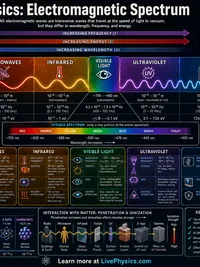
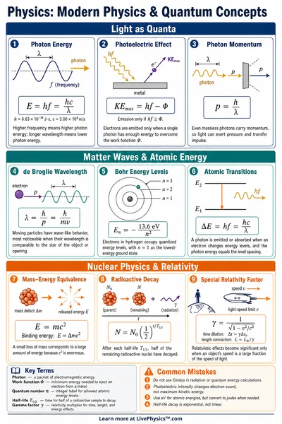
- The emitted photon energy equals the band gap, so a wider gap gives bluer light and a narrower gap gives redder or infrared light.
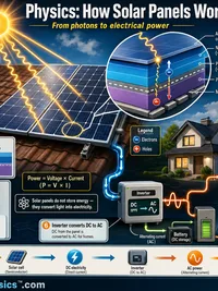
- A gap near 1.1 to 1.5 eV captures the most sunlight in a single junction, which is why silicon and gallium arsenide dominate solar cells.
Reference Guide
Energy bands and the band gap
In a solid, atomic energy levels spread into bands. The valence band holds the bonding electrons and the conduction band holds the electrons that are free to move. Between them lies a range of energies that electrons cannot occupy.
That range is the band gap, written Eg. A small gap means electrons jump to the conduction band easily, so the material conducts. A large gap means few electrons make the jump, so the material behaves more like an insulator.
- Silicon Eg is about 1.12 eV at room temperature.
- Germanium has a smaller gap of about 0.66 eV.
- Gallium nitride has a wide gap near 3.4 eV.
Temperature and intrinsic carriers
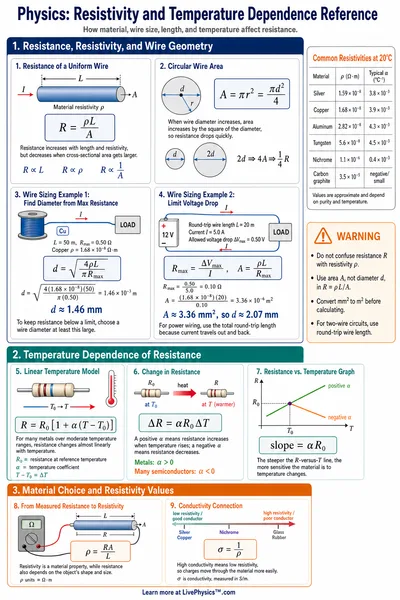
The band gap shrinks as a crystal heats up because the lattice expands and atoms vibrate more. The Varshni equation captures this, Eg(T) = Eg0 minus alpha times T squared over T plus beta.
Heat also frees more electrons. The intrinsic carrier concentration ni rises steeply with temperature, since it follows an exponential of minus Eg over twice kT. A 100 K rise can raise ni by orders of magnitude.
This is why a small gap material like germanium leaks current at high temperature and why silicon devices are derated as they get hot.
Doping, the Fermi level, and conductivity
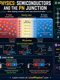
Doping adds impurity atoms that donate electrons (n-type) or accept them, leaving holes (p-type). One carrier type then dominates, raising conductivity by orders of magnitude over the pure crystal.
The Fermi level marks the energy where states are half filled. N-type doping pushes it up toward the conduction band, p-type doping pulls it down toward the valence band. The band diagram shows this as the dashed line moving inside the gap.
Conductivity is q times n times electron mobility plus p times hole mobility, so both the carrier count and how freely carriers move matter.
Band gap to LED color and solar cells
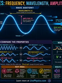
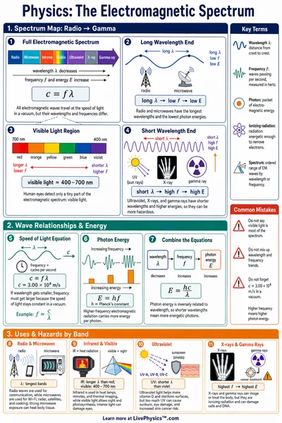
When an electron drops from the conduction band to the valence band, it can emit a photon whose energy equals the gap. The wavelength is hc over Eg, so a wider gap gives bluer light and a narrow gap gives red or infrared light.
- Direct-gap materials such as GaAs and GaN emit light efficiently and make good LEDs.
- Indirect-gap materials such as silicon are poor emitters because recombination needs a phonon.
- A gap near 1.1 to 1.5 eV best matches the solar spectrum for a single junction.
This is why silicon and gallium arsenide are the workhorses of photovoltaics while nitrides power blue and white LEDs.